Sources for defining custom PCB shapes
-
Hi guys,
Hoping all are staying safe and healthy. I am using Altium for designing my PCB's. Although altium sources an option for designing custom PCB shapes, It is not so accurate. So, I want to use softwares to design my shape and import it as .DXF or .DWG file to altium. I have know that Solid works is one such kind of software.
But, I wanna know whether there are any online tools for designing this?
-
Hi @kowshik1729 , There is many CAD software that supports .DXF format and it's very simple to generate one, I'll list some of the online tools below and may I know why you want to use the online tools?
-
@salmanfaris Thanks. The reason I wanna use online tools only is because, I have been using my company's lappy and I am restricted to install any other Softwares. So, online tools will be an easy way for me. by the way I have found another way too. EasyEDA provides an super easy solution for creating custom PCB shapes. It really came in handy for me.
-
@kowshik1729 Glad to hear that!
 so you're exporting the dxf/ board file from the EasyEDA? can you explain the process?
 -
@salmanfaris Sure I can.
-
Open easyEDA and open an empty PCB project.
-
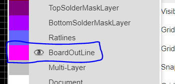
On the top right corner you can find the layer selection . Selection "Board Outline" alone to make it active layer. The eye symbol and pencil symbol must be on the same layer.
-
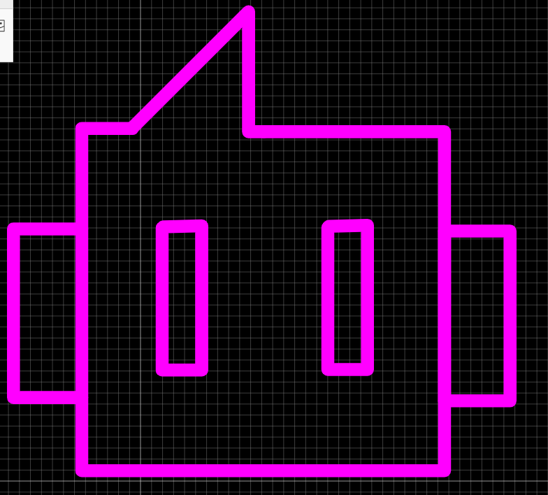
Now, you can draw any shape by using the tools available on the screen. They look something as shown below,

-
I made makergram shape as shown below.
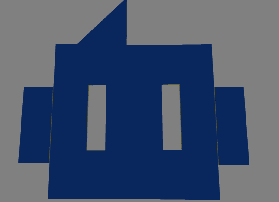
- It even offers a 3D view where you can get by clicking on the camera symbol in the toolbar.
- Click on "File" menu and click on "Export" and click ".DXF" format. This will download DXF file which you can put it up in your CAD software.
And lastly, all these shape creations is done in less than 10 minutes which is very much time efficient and easy to incorporate to your designs.
-
-
That's cool
 , nice hacky solution. Thanks for sharing detailed instruction, @kowshik1729. for me it was done by syncing the eagle and fusion360, create board layout in the fusion360 as PCB Profile and Import the layout from fusion360 to the eagle.
 -
@salmanfaris I see. That looks as an effecient solution too. I'll try it out this time.

-
The reason I wanna use online tools only is because, I have been using my company's lappy and I am restricted to install any other Softwares. So, online tools will be an easy way for me. by the way I have found another way too. EasyEDA provides an super easy solution for creating custom PCB shapes. It really came in handy for me.
Recent Posts
-

Hi all,
I recently came across this post where they have shown photos printed on PCB in high resolution. I would like to know how to add this kind of photos to the silkscreen layers of the PCB in Eagle/Altium.
Adding such kind of photos will be attractive for beginners and also can be used for educational purposes too.
Please let me know in case anybody knows. -

@kowshik1729 I think that might not get since the platform is not opensource! but they provided everything you need to develop a system with that.
-

@kowshik1729 Carrier board schematics for SoMs will be always available as they need to be modified as per customer application, however SoM design files are hard to get unless the H/W design is truly open-source.
-
@salmanfaris Actually the schematics files you've mentioned are the same files which I've got from them. They are carrier board design files.
