• Categories
  • Recent
  • Popular
  • Tags
  • Users
  • Groups
  • Register
  • Login
MakerGram Logo

MakerGram

  • Register
  • Login
  • Search
  • Categories
  • Recent
  • Popular
  • Tags
  • Users
  • Groups

Day 3: Create Board layout from Schematics

RSET PCB Designing Workshop
4
5
685
Loading More Posts
  • Oldest to Newest
  • Newest to Oldest
  • Most Votes
Reply
  • Reply as topic
Log in to reply
This topic has been deleted. Only users with topic management privileges can see it.
  • salmanfaris
    salmanfaris last edited by salmanfaris 24 Mar 2020, 06:48 24 Mar 2020, 06:47

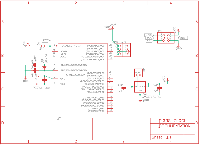
    Yesterday we created the DigitalClock Schematics and today we are convert the Schematics into Board layout and complete the PCB Design.

    ToDo:

    • Design your own board from your Schematics file

    • Document and share here.

    D 1 Reply Last reply 25 Mar 2020, 14:11 Reply Quote 1
    • salmanfaris
      salmanfaris last edited by 24 Mar 2020, 06:48

      clock.png

      1 Reply Last reply Reply Quote 0
      • hisham
        hisham last edited by 25 Mar 2020, 07:31

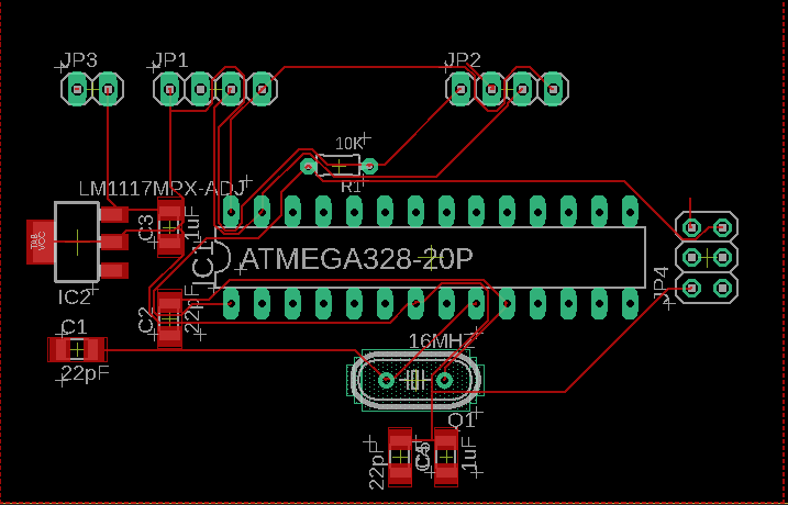
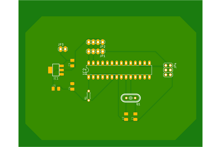
        Created board layout for Atmega based digital clock on attending the online workshop on Autodesk Eagle by @salmanfaris .
        Didital_clock.png

        1 Reply Last reply Reply Quote 1
        • D
          Daniel Hardly @salmanfaris last edited by 25 Mar 2020, 14:11

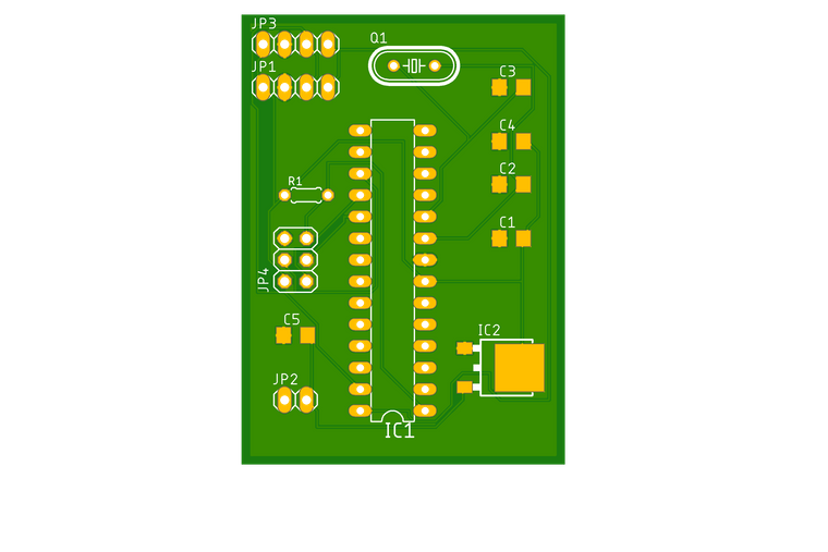
          PCB DESIGN DIGITAL CLOCK
          DIGITAL CLOCK.png
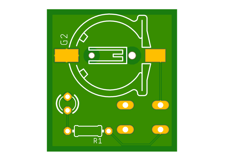
          SIMPLE LED
          first pcb.png

          1 Reply Last reply Reply Quote 2
          • G
            Ggreeshma stani last edited by 31 Mar 2020, 20:08

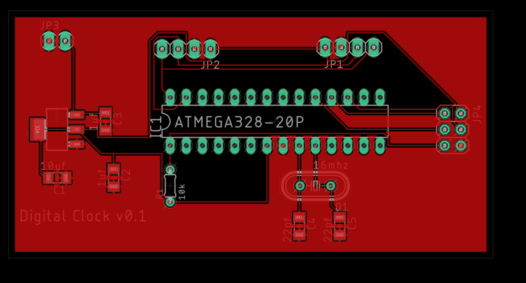
            Created board layout for Atmega based digital clock on attending the online workshop on Autodesk Eaglefirst project.PNG first.PNG CLASS1.png

            1 Reply Last reply Reply Quote 1
            1 out of 5
            • First post
              1/5
              Last post

            Recent Posts

            • @Ggreeshma-stani Pretty good than the previous design. I am able to see 2 crystals on the board. Can I know why did you use another one?

              And finally, you can address me as kowshik. No need of sir😉

              7 Apr 2020, 08:20 • read more
            • G

              @salmanfaris yes sir i have made the changes and have minimised the board size.

              6 Apr 2020, 17:03 • read more
            • G

              @kowshik1729 sir i have made the appropriate corrections.
              and thank you for notifying me on the errors

              6 Apr 2020, 17:02 • read more
            • @hisham Ahaaa...!! Looks like you've fixed the error. Great job.

              We'll be glad to have a look once your PCB is fabricated...😉

              3 Apr 2020, 18:16 • read more
            • @hisham also make sure Design Rules are matching with our manufacture capabilities! In this case, we are planned to use Seeed Studio Fusion PCB Service, so you can check their PCB capabilities and configure your PCB Design Rules.

              Fusion PCB Specification

              3 Apr 2020, 17:58 • read more
            By MakerGram | A XiStart Initiative | Built with ♥ NodeBB
            Copyright © 2023 MakerGram, All rights reserved.
            Privacy Policy | Terms & Conditions | Disclaimer | Code of Conduct